M.Tech U-I Atomic and molecular basics
Intermolecular and intramolecular forces-1
Unit-I Atomic and Molecular Basics: The scope, The nanoscale systems, Defining nano dimensional materials, Size effects in nano materials, Application and technology development, General methods available for the synthesis of nano dimensional materials.
Particles and Bonds, Chemical bonds in Nano technology, The shapes of molecules, additional aspects of bonding, Molecular geometry: VSEPR Model, Hybridization, Van der Waals interactions, Dipole–Dipole Interactions, Ionic Interactions, Metal bonds, Covalent bonds, Coordinative bonds, Hydrogen bridge bonds and polyvalent bonds.
Nanotechnology is science, engineering, and technology conducted at the nanoscale, which is about 1 to 100 nanometers.
 |
| Physicist Richard Feynman, the father of nanotechnology. |
Nanoscience and nanotechnology are the study and application of extremely small things and can be used across all the other science fields, such as chemistry, biology, physics, materials science, and engineering.
The ideas and concepts behind nanoscience and nanotechnology started with a talk entitled “There’s Plenty of Room at the Bottom” by physicist Richard Feynman at an American Physical Society meeting at the California Institute of Technology (CalTech) on December 29, 1959, long before the term nanotechnology was used. In his talk, Feynman described a process in which scientists would be able to manipulate and control individual atoms and molecules. Over a decade later, in his explorations of ultraprecision machining, Professor Norio Taniguchi coined the term nanotechnology. It wasn’t until 1981, with the development of the scanning tunneling microscope that could “see” individual atoms, that modern nanotechnology began.
 |
|
| Medieval stained glass windows are an example of how nanotechnology was used in the pre-modern era. (Courtesy: NanoBioNet) |
It’s hard to imagine just how small nanotechnology is. One nanometer is a billionth of a meter, or 10-9 of a meter. Here are a few illustrative examples:
- There are 25,400,000 nanometers in an inch
- A sheet of newspaper is about 100,000 nanometers thick
- On a comparative scale, if a marble were a nanometer, then one meter would be the size of the Earth
Nanoscience and nanotechnology involve the ability to see and to control individual atoms and molecules. Everything on Earth is made up of atoms—the food we eat, the clothes we wear, the buildings and houses we live in, and our own bodies.
But something as small as an atom is impossible to see with the naked eye. In fact, it’s impossible to see with the microscopes typically used in a high school science classes. The microscopes needed to see things at the nanoscale were invented relatively recently—about 30 years ago.
Once scientists had the right tools, such as the scanning tunneling microscope (STM) and the atomic force microscope (AFM), the age of nanotechnology was born.
Although modern nanoscience and nanotechnology are quite new, nanoscale materials were used for centuries. Alternate-sized gold and silver particles created colors in the stained glass windows of medieval churches hundreds of years ago. The artists back then just didn’t know that the process they used to create these beautiful works of art actually led to changes in the composition of the materials they were working with.
Today’s scientists and engineers are finding a wide variety of ways to deliberately make materials at the nanoscale to take advantage of their enhanced properties such as higher strength, lighter weight, increased control of light spectrum, and greater chemical reactivity than their larger-scale counterparts.
What is Nanotechnology?
| Nanotechnology is the engineering of functional systems at the molecular scale. This covers both current work and concepts that are more advanced.In its original sense, ‘nanotechnology’ refers to the projected ability to construct items from the bottom up, using techniques and tools being developed today to make complete, high performance products. |
With 15,342 atoms, this parallel-shaft speed reducer gear is one of the largest nanomechanical devices ever modeled in atomic detail. LINK |
The Meaning of Nanotechnology
When K. Eric Drexler (right) popularized the word ‘nanotechnology’ in the 1980’s, he was talking about building machines on the scale of molecules, a few nanometers wide—motors, robot arms, and even whole computers, far smaller than a cell. Drexler spent the next ten years describing and analyzing these incredible devices, and responding to accusations of science fiction. Meanwhile, mundane technology was developing the ability to build simple structures on a molecular scale. As nanotechnology became an accepted concept, the meaning of the word shifted to encompass the simpler kinds of nanometer-scale technology. The U.S. National Nanotechnology Initiative was created to fund this kind of nanotech: their definition includes anything smaller than 100 nanometers with novel properties.
Much of the work being done today that carries the name ‘nanotechnology’ is not nanotechnology in the original meaning of the word. Nanotechnology, in its traditional sense, means building things from the bottom up, with atomic precision. This theoretical capability was envisioned as early as 1959 by the renowned physicist Richard Feynman.
I want to build a billion tiny factories, models of each other, which are manufacturing simultaneously. . . The principles of physics, as far as I can see, do not speak against the possibility of maneuvering things atom by atom. It is not an attempt to violate any laws; it is something, in principle, that can be done; but in practice, it has not been done because we are too big. — Richard Feynman, Nobel Prize winner in physics
Based on Feynman’s vision of miniature factories using nanomachines to build complex products, advanced nanotechnology (sometimes referred to as molecular manufacturing) will make use of positionally-controlled mechanochemistry guided by molecular machine systems. Formulating a roadmap for development of this kind of nanotechnology is now an objective of a broadly basedtechnology roadmap project led by Battelle (the manager of several U.S. National Laboratories) and the Foresight Nanotech Institute.
Shortly after this envisioned molecular machinery is created, it will result in a manufacturing revolution, probably causing severe disruption. It also has serious economic, social, environmental, and military implications.
Four Generations
Mihail (Mike) Roco of the U.S. National Nanotechnology Initiative has described four generations of nanotechnology development (see chart below). The current era, as Roco depicts it, is that of passive nanostructures, materials designed to perform one task. The second phase, which we are just entering, introduces active nanostructures for multitasking; for example, actuators, drug delivery devices, and sensors. The third generation is expected to begin emerging around 2010 and will feature nanosystems with thousands of interacting components. A few years after that, the first integrated nanosystems, functioning (according to Roco) much like a mammalian cell with hierarchical systems within systems, are expected to be developed.
Some experts may still insist that nanotechnology can refer to measurement or visualization at the scale of 1-100 nanometers, but a consensus seems to be forming around the idea (put forward by the NNI’s Mike Roco) that control and restructuring of matter at the nanoscale is a necessary element. CRN’s definition is a bit more precise than that, but as work progresses through the four generations of nanotechnology leading up to molecular nanosystems, which will include molecular manufacturing, we think it will become increasingly obvious that “engineering of functional systems at the molecular scale” is what nanotech is really all about.
Conflicting Definitions
Unfortunately, conflicting definitions of nanotechnology and blurry distinctions between significantly different fields have complicated the effort to understand the differences and develop sensible, effective policy.
The risks of today’s nanoscale technologies (nanoparticle toxicity, etc.) cannot be treated the same as the risks of longer-term molecular manufacturing (economic disruption, unstable arms race, etc.). It is a mistake to put them together in one basket for policy consideration—each is important to address, but they offer different problems and will require different solutions. As used today, the term nanotechnology usually refers to a broad collection of mostly disconnected fields. Essentially, anything sufficiently small and interesting can be called nanotechnology. Much of it is harmless. For the rest, much of the harm is of familiar and limited quality. But as we will see, molecular manufacturing will bring unfamiliar risks and new classes of problems.
General-Purpose Technology
Nanotechnology is sometimes referred to as a general-purpose technology. That’s because in its advanced form it will have significant impact on almost all industries and all areas of society. It will offer better built, longer lasting, cleaner, safer, and smarter products for the home, for communications, for medicine, for transportation, for agriculture, and for industry in general.
Imagine a medical device that travels through the human body to seek out and destroy small clusters of cancerous cells before they can spread. Or a box no larger than a sugar cube that contains the entire contents of the Library of Congress. Or materials much lighter than steel that possess ten times as much strength. — U.S. National Science Foundation
Dual-Use Technology
Like electricity or computers before it, nanotech will offer greatly improved efficiency in almost every facet of life. But as a general-purpose technology, it will be dual-use, meaning it will have many commercial uses and it also will have many military uses—making far more powerful weapons and tools of surveillance. Thus it represents not only wonderful benefits for humanity, but also grave risks.
A key understanding of nanotechnology is that it offers not just better products, but a vastly improved manufacturing process. A computer can make copies of data files—essentially as many copies as you want at little or no cost. It may be only a matter of time until the building of products becomes as cheap as the copying of files. That’s the real meaning of nanotechnology, and why it is sometimes seen as “the next industrial revolution.”
My own judgment is that the nanotechnology revolution has the potential to change America on a scale equal to, if not greater than, the computer revolution. — U.S. Senator Ron Wyden (D-Ore.)
The power of nanotechnology can be encapsulated in an apparently simple device called a personal nanofactory that may sit on your countertop or desktop. Packed with miniature chemical processors, computing, and robotics, it will produce a wide-range of items quickly, cleanly, and inexpensively, building products directly from blueprints.
Exponential Proliferation
Nanotechnology not only will allow making many high-quality products at very low cost, but it will allow making new nanofactories at the same low cost and at the same rapid speed. This unique (outside of biology, that is) ability to reproduce its own means of production is why nanotech is said to be an exponential technology. It represents a manufacturing system that will be able to make more manufacturing systems—factories that can build factories—rapidly, cheaply, and cleanly. The means of production will be able to reproduce exponentially, so in just a few weeks a few nanofactories conceivably could become billions. It is a revolutionary, transformative, powerful, and potentially very dangerous—or beneficial—technology.
How soon will all this come about? Conservative estimates usually say 20 to 30 years from now, or even much later than that. However, CRN is concerned that it may occur sooner, quite possibly within the next decade. This is because of the rapid progress being made in enabling technologies, such as optics, nanolithography, mechanochemistry and 3D prototyping. If it does arrive that soon, we may not be adequately prepared, and the consequences could be severe.
We believe it’s not too early to begin asking some tough questions and facing the issues:
| Who will own the technology? | |
| Will it be heavily restricted, or widely available? | |
| What will it do to the gap between rich and poor? | |
| How can dangerous weapons be controlled, and perilous arms races be prevented? |
Many of these questions were first raised over a decade ago, and have not yet been answered. If the questions are not answered with deliberation, answers will evolve independently and will take us by surprise; the surprise is likely to be unpleasant.
It is difficult to say for sure how soon this technology will mature, partly because it’s possible (especially in countries that do not have open societies) that clandestine military or industrial development programs have been going on for years without our knowledge.
We cannot say with certainty that full-scale nanotechnology will not be developed with the next ten years, or even five years. It may take longer than that, but prudence—and possibly our survival—demands that we prepare now for the earliest plausible development scenario.
Nanoscale
Nanoscale particles are not new in either nature or science. However, the recent leaps in areas such as microscopy have given scientists new tools to understand and take advantage of phenomena that occur naturally when matter is organized at the nanoscale. In essence, these phenomena are based on “quantum effects“ and other simple physical effects such as expanded surface area (more on these below). In addition, the fact that a majority of biological processes occur at the nanoscale gives scientists models and templates to imagine and construct new processes that can enhance their work in medicine, imaging, computing, printing, chemical catalysis, materials synthesis, and many other fields. Nanotechnology is not simply working at ever smaller dimensions; rather, working at the nanoscale enables scientists to utilize the unique physical, chemical, mechanical, and optical properties of materials that naturally occur at that scale.
 |
| Computer simulation of electron motions within a nanowire that has a diameter in the nanoscale range. |
When particle sizes of solid matter in the visible scale are compared to what can be seen in a regular optical microscope, there is little difference in the properties of the particles. But when particles are created with dimensions of about 1–100 nanometers (where the particles can be “seen” only with powerful specialized microscopes), the materials’ properties change significantly from those at larger scales. This is the size scale where so-called quantum effects rule the behavior and properties of particles. Properties of materials are size-dependent in this scale range. Thus, when particle size is made to be nanoscale, properties such as melting point, fluorescence, electrical conductivity, magnetic permeability, and chemical reactivity change as a function of the size of the particle.
Nanoscale gold illustrates the unique properties that occur at the nanoscale. Nanoscale gold particles are not the yellow color with which we are familiar; nanoscale gold can appear red or purple. At the nanoscale, the motion of the gold’s electrons is confined. Because this movement is restricted, gold nanoparticles react differently with light compared to larger-scale gold particles. Their size and optical properties can be put to practical use: nanoscale gold particles selectively accumulate in tumors, where they can enable both precise imaging and targeted laser destruction of the tumor by means that avoid harming healthy cells.
A fascinating and powerful result of the quantum effects of the nanoscale is the concept of “tunability” of properties. That is, by changing the size of the particle, a scientist can literally fine-tune a material property of interest (e.g., changing fluorescence color; in turn, the fluorescence color of a particle can be used to identify the particle, and various materials can be “labeled” with fluorescent markers for various purposes). Another potent quantum effect of the nanoscale is known as“tunneling,” which is a phenomenon that enables the scanning tunneling microscope and flash memory for computing.
Over millennia, nature has perfected the art of biology at the nanoscale. Many of the inner workings of cells naturally occur at the nanoscale. For example, hemoglobin, the protein that carries oxygen through the body, is 5.5 nanometers in diameter. A strand of DNA, one of the building blocks of human life, is only about 2 nanometers in diameter.
Drawing on the natural nanoscale of biology, many medical researchers are working on designing tools, treatments, and therapies that are more precise and personalized than conventional ones—and that can be applied earlier in the course of a disease and lead to fewer adverse side-effects. One medical example of nanotechnology is the bio-barcode assay, a relatively low-cost method of detecting disease-specific biomarkers in the blood, even when there are very few of them in a sample. The basic process, which attaches “recognition” particles and DNA “amplifiers” to gold nanoparticles, was originally demonstrated at Northwestern University for a prostate cancer biomarker following prostatectomy. The bio-barcode assay has proven to be considerably more sensitive than conventional assays for the same target biomarkers, and it can be adapted to detect almost any molecular target.i
Growing understanding of nanoscale biomolecular structures is impacting other fields than medicine. Some scientists are looking at ways to use nanoscale biological principles of molecular self-assembly, self-organization, and quantum mechanics to create novel computing platforms. Other researchers have discovered that in photosynthesis, the energy that plants harvest from sunlight is nearly instantly transferred to plant “reaction centers” by quantum mechanical processes with nearly 100% efficiency (little energy wasted as heat). They are investigating photosynthesis as a model for “green energy” nanosystems for inexpensive production and storage of nonpolluting solar power.ii
Nanoscale materials have far larger surface areas than similar masses of larger-scale materials. As surface area per mass of a material increases, a greater amount of the material can come into contact with surrounding materials, thus affecting reactivity.
A simple thought experiment shows why nanoparticles have phenomenally high surface areas. A solid cube of a material 1 cm on a side has 6 square centimeters of surface area, about equal to one side of half a stick of gum. But if that volume of 1 cubic centimeter were filled with cubes 1 mm on a side, that would be 1,000 millimeter-sized cubes (10 x 10 x 10), each one of which has a surface area of 6 square millimeters, for a total surface area of 60 square centimeters—about the same as one side of two-thirds of a 3” x 5” note card. When the 1 cubic centimeter is filled with micrometer-sized cubes—a trillion (1012) of them, each with a surface area of 6 square micrometers—the total surface area amounts to 6 square meters, or about the area of the main bathroom in an average house. And when that single cubic centimeter of volume is filled with 1-nanometer-sized cubes—1021 of them, each with an area of 6 square nanometers—their total surface area comes to 6,000 square meters. In other words, a single cubic centimeter of cubic nanoparticles has a total surface area one-third larger than a football field!
 |
| Illustration demonstrating the effect of the increased surface area provided by nanostructured materials |
One benefit of greater surface area—and improved reactivity—in nanostructured materials is that they have helped create better catalysts. As a result, catalysis by engineered nanostructured materials already impacts about one-third of the huge U.S.—and global—catalyst markets, affecting billions of dollars of revenue in the oil and chemical industries.iii An everyday example of catalysis is the catalytic converter in a car, which reduces the toxicity of the engine’s fumes. Nanoengineered batteries, fuel cells, and catalysts can potentially use enhanced reactivity at the nanoscale to produce cleaner, safer, and more affordable modes of producing and storing energy.
Large surface area also makes nanostructured membranes and materials ideal candidates for water treatment and desalination (e.g., see “Self-Assembled, Nanostructured Carbon for Energy Storage and Water Treatment” in our database,NNI Accomplishments Archive), among other uses. It also helps support “functionalization” of nanoscale material surfaces (adding particles for specific purposes), for applications ranging from drug delivery to clothing insulation.
Synthesis of Nanomaterials
It is classified as bottom-up manufacturing which involves building up of the atom or molecular constituents as against the top method which involves making smaller and smaller structures through etching from the bulk material as exemplified by the semiconductor industry.
Gas Condensation
Gas condensation was the first technique used to synthesize nanocrystalline metals and alloys. In this technique, a metallic or inorganic material is vaporized using thermal evaporation sources such as a Joule heated refractory crucibles, electron beam evaporation devices, in an atmosphere of 1-50 m bar. In gas evaporation, a high residual gas pressure causes the formation of ultra fine particles (100 nm) by gas phase collision. The ultrafiine particles are formed by collision of evaporated atoms with residual gas molecules. Gas pressures greater than 3 mPa (10 torr) are required. Vaporization sources may be resistive heating, high energy electron beams, low energy electron beam and inducting heating. Clusters form in the vicinity of the source by homogenous nucleation in the gas phase grew by incorporation by atoms in the gas phase. It comprises of a ultra high vacuum (UHV) system fitted evaporation source, a cluster collection device of liquid nitrogen filled cold finger scrapper assembly and compaction device. During heating, atoms condense in the supersaturation zone close to Joule heating device. The nanoparticles are removed by scrapper in the form of a metallic plate. Evaporation is to be done from W, Ta or Mo refractory metal crucibles. If the metals react with crucibles, electron beam evaporation technique is to be used. The method is extremely slow. The method suffers from limitations such as a source-precursor incompatibility, temperature ranges and dissimilar evaporation rates in an alloy. Alternative sources have been developed over the years. For instance, Fe is evaporated into an inert gas atmosphere (He). Through collision with the atoms the evaporated Fe atoms loose kinetic energy and condense in the form of small crystallite crystals, which accumulate as a loose powder. Sputtering or laser evaporation may be used instead of thermal evaporation. Sputtering is a non-thermal process in which surface atoms are physically ejected from the surface by momentum transfer from an energetic bombarding species of atomic/molecular size. Typical sputtering uses a glow discharge or ion beam. Interaction events which occur at and near the target surface during the sputtering process in magnetron sputtering has advantage over diode and triode sputtering. In magnetron sputtering, most of the plasma is confined to the near target region. Other alternate energy sources which have been successfully used to produce clusters or ultra fine particles are sputtering electron beam heating and plasma methods. Sputtering has been used in low pressure environment to produce a variety of clusters including Ag, Fe and Si.
Vacuum Deposition and Vaporization
Before proceeding to the other methods, it is important to understand the terms vacuum deposition and vaporization or vacuum evaporation. In vacuum deposition process, elements, alloys or compounds are vaporized and deposited in a vacuum . The vaporization source is the one that vaporizes materials by thermal processes. The process is carried out at pressure of less than 0.1 Pa (1 m Torr) and in vacuum levels of 10 to 0.1 MPa. The substrate temperature ranges from ambient to 500°C. The saturation or equilibrium vapor pressure of a material is defined as the vapor pressure of the material in equilibrium with the solid or liquid surface. For vacuum deposition, a reasonable deposition rate can be obtained if the vaporization rate is fairly high. A useful deposition rate is obtained at a vapor pressure of 1.3 Pa (0.01 Torr).
Vapor phase nucleation can occur in dense vapor cloud by multibody collisions, The atoms are passed through a gas to provide necessary collision and cooling for nucleation. These particles are in the range of 1 to 100 nm and are called ultra fine particles or clusters. The advantages associated with vacuum deposition process are high deposition rates and economy. However, the deposition of many compounds is difficult. Nanoparticles produced from a supersaturated vapor are usually longer than the cluster.
Chemical Vapor Deposition (CVD) and Chemical Vapor Condensation (CVC)
CVD is a well known process in which a solid is deposited on a heated surface via a chemical reaction from the vapor or gas phase. CVC reaction requires activation energy to proceed. This energy can be provided by several methods. In thermal CVD the reaction is activated by a high temperature above 900oC. A typical apparatus comprises of gas supply system, deposition chamber and an exhaust system. In plasma CVD, the reaction is activated by plasma at temperatures between 300 and 700°C. In laser CVD, pyrolysis occurs when laser thermal energy heats an absorbing substrate. In photo-laser CVD, the chemical reaction is induced by ultra violet radiation which has sufficient photon energy, to break the chemical bond in the reactant molecules. In this process, the reaction is photon activated and deposition occurs at room temperature. Nano composite powders have been prepared by CVD. SiC/Si3N composite powder was prepared using SiH4, CH4, WF6 and H2 as a source of gas at 1400°C. Another process called chemical vapor condensation (CVC) was developed in Germany in 1994. It involves pyrolysis of vapors of metal organic precursors in a reduced pressure atmosphere. Particles of ZrO2, Y2O3 and nanowhiskers have been produced by CVC method. A metalorganic precursor is introduced in the hot zone of the reactor using mass flow controller. For instance, hexamethyldisilazane (CH3)3 Si NHSi (CH3)3 was used to produce SiCxNyOz powder by CVC technique. The reactor allows synthesis of mixtures of nanoparticles of two phases or doped nanoparticles by supplying two precursors at the front end of reactor and coated nanoparticles, n-ZrO2, coated with n-Al2O3 by supplying a second precursor in a second stage of reactor. The process yields quantities in excess of 20 g/hr. The yield can be further improved by enlarging the diameter of hot wall reactor and mass of fluid through the reactor. Typical nanocrystalline materials which have been synthesized are shown in Table 1.
Table 1. Typical nanocrystalline materials synthesized by the CVC method
| Precursor | Product Powder | Phase as prepared |
Average Particle size (nm) | Surface Area (m2/g) |
| (CH3) 3SiNHSi(CH3) 3 | SiCxNyOz | Amorphous | 4 | 377 |
| Si(CH3)4 | SiC | β-phase | 9 | 201 |
| Al[2-OC4H9]3 | Al2O3 | Amorphous | 3.5 | 449 |
| Ti[I-OC3H7]4 | TiO2 | Anatase | 8 | 193 |
| Si[OC2H5]4 | SiO2 | Amorphous | 6 | 432 |
| Zr[3-OC4H9]4 | ZrO2 | Monoclinic | 7 | 134 |
Mechanical Attrition
Unlike many of the methods mentioned above, mechanical attrition produces its nanostructures not by cluster assembly but by the structural decomposition of coarser grained structures as a result of plastic deformation. Elemental powders of Al and β-SiC were prepared in a high energy ball mill. More recently, ceramic/ceramic nanocomposite WC-14% MgO material has been fabricated. The ball milling and rod milling techniques belong to the mechanical alloying process which has received much attention as a powerful tool for the fabrication of several advanced materials. Mechanical alloying is a unique process, which can be carried out at room temperature. The process can be performed on both high energy mills, centrifugal type mill and vibratory type mill, and low energy tumbling mill.
Examples of High Energy Mills
High energy mills include:
- Attrition Ball Mill
- Planetary Ball Mill
- Vibrating Ball Mill
- Low Energy Tumbling Mill
- High Energy Ball Mill
Attrition Ball Mill
The milling procedure takes place by a stirring action of a agitator which has a vertical rotator central shaft with horizontal arms (impellers). The rotation speed was later increased to 500 rpm. Also, the milling temperature was in greater control.
Planetary Ball Mill
Centrifugal forces are caused by rotation of the supporting disc and autonomous turning of the vial. The milling media and charge powder alternatively roll on the inner wall of the vial and are thrown off across the bowl at high speed (360 rpm).
Vibrating Ball Mill
It is used mainly for production of amorphous alloys. The changes of powder and milling tools are agitated in the perpendicular direction at very high speed (1200 rpm).
Low Energy Tumbling Mill
They have been used for successful preparation of mechanically alloyed powder. They are simple to operate with low operation costs. A laboratory scale rod mill was used to prepare homogenous amorphous Al30Ta70 powder by using S.S. cylinder rods. Single-phase amorphous powder of AlxTm100-x with low iron concentration can be formed by this technique.
High Energy Ball Mill
High-energy ball milling is an already established technology, however, it has been considered dirty because of contamination problems with iron. However, the use of tungsten carbide component and inert atmosphere and /or high vacuum processes has reduced impurity levels to within acceptable limits. Common drawbacks include low surface, highly poly disperse size distribution, and partially amorphous state of the powder. These powders are highly reactive with oxygen, hydrogen and nitrogen. Mechanical alloying leads to the fabrication of alloys, which cannot be produced by conventional techniques. It would not be possible to produce an alloy of Al-Ta, because of the difference in melting points of Al (933 K) and Ta (3293 K) by any conventional process. However, it can be fabricated by mechanical alloying using ball milling process.
Other Processes
Several other processes such as hydrodynamic cavitation micro emulsion and sonochemical processing techniques have also been used. In cavitation process nanoparticles are generated through creation and release of gas bubbles inside the sol-gel solution. By pressurizing in super critical drying chamber and exposing to cavitational disturbances and high temperature heating, the sol-gel is mixed. Te erupted hydrodynamic bubbles cause the nucleation, growth and quenching of nanoparticles. Particle size can be controlled by adjusting pressure and solution retention times.
Sol-Gel Techniques
In addition to techniques mentioned above, the sol-gel processing techniques have also been extensively used. Colloidal particles are much larger than normal molecules or nanoparticles. However, upon mixing with a liquid colloids appear bulky whereas the nanosized molecules always look clear. It involves the evolution of networks through the formation of colloidal suspension (sol) and gelatin to form a network in continuous liquid phase (gel). The precursor for synthesizing these colloids consists of ions of metal alkoxides and aloxysilanes. The most widely used are tetramethoxysilane (TMOS), and tetraethoxysilanes (TEOS) which form silica gels. Alkoxides are immiscible in water. They are organo metallic precursors for silica, aluminum, titanium, zirconium and many others. Mutual solvent alcohol is used. The sol gel process involves initially a homogeneous solution of one or more selected alkoxides. These are organic precursors for silica, alumina, titania, zirconia, among others. A catalyst is used to start reaction and control pH. Sol-gel formation occurs in four stages.
- Hydrolysis
- Condensation
- Growth of particles
- Agglomeration of particles
Hydrolysis
During hydrolysis, addition of water results in the replacement of [OR] group with [OH-] group. Hydrolysis occurs by attack of oxygen on silicon atoms in silica gel. Hydrolysis can be accelerated by adding a catalyst such as HCl and NH3. Hydrolysis continues until all alkoxy groups are replaced by hydroxyl groups. Subsequent condensation involving silanol group (Si-OH) produced siloxane bonds (Si-O-Si) and alcohol and water. Hydrolysis occurs by attack of oxygen contained in the water on the silicon atom.
Condensation
Polymerization to form siloxane bond occurs by either a water producing or alcohol producing condensation reaction. The end result of condensation products is the formation of monomer, dimer, cyclic tetramer, and high order rings. The rate of hydrolysis is affected by pH, reagent concentration and H2O/Si molar ratio (in case of silica gels). Also ageing and drying are important. By control of these factors, it is possible to vary the structure and properties of sol-gel derived inorganic networks.
Growth and Agglomeration
As the number of siloxane bonds increase, the molecules aggregate in the solution, where they form a network, a gel is formed upon drying. The water and alcohol are driven off and the network shrinks. At values of pH of greater then 7, and H2O/Si value ranging from 7 to 5. Spherical nano-particles are formed. Polymerization to form siloxane bonds by either an alcohol producing or water producing condensate occurs.
2 HOSi (OR)3 → (OR)3 Si O Si (OR)3 + H2O
or
2 HOSi (OR) 3 → (OR)2OH Si O Si (OR)3 + H2O
Above pH of 7, Silica is more soluble and silica particles grow in size. Growth stops when the difference in solubility between the smallest and largest particles becomes indistinguishable. Larger particles are formed at higher temperatures. Zirconium and Yttrium gels can be similarly produced.
Despite improvements in both chemical and physical methods of synthesis, there remain some problems and limitations. Laser vaporization technique has offered several advantages over other heating techniques. A high energy pulsed laser with an intensity flux of 106 – 107 W/cm2 is forced on target material. The plasma causes high vaporization and high temperature (10,000°C). Typical yields are 1014-1015 atoms from the surface area of 0.01 cm2 in a 10-8 s pulse. Thus a high density of vapor is produced in a very short time (10-8 s), which is useful for direct deposition of particles.
Electrodeposition
Nanostructured materials can also be produced by electrodeposition. These films are mechanically strong, uniform and strong. Substantial progress has been made in nanostructured coatings applied either by DVD or CVD. Many other non-conventional processes such as hypersonic plasma particle deposition (HPPD) have been used to synthesize and deposit nanoparticles. The significant potential of nanomaterial synthesis and their applications is virtually unexplored. They offer numerous challenges to overcome. Understanding more of synthesis would help in designing better materials. It has been shown that certain properties of nanostructured deposits such as hardness, wear resistance and electrical resistivity are strongly affected by grain size. A combination of increased hardness and wear resistance results in a superior coating performance.
CHEMICAL BOND IN NANOTECHNOLOGY
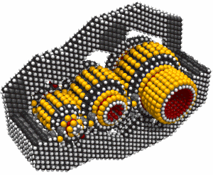
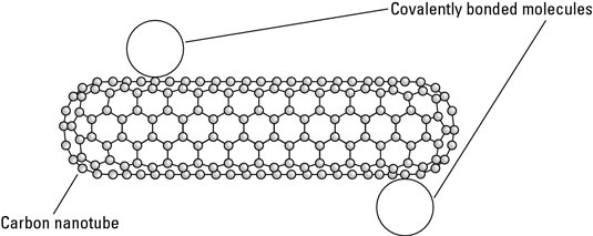
The properties of nanoparticles can be customized for use in a particular nanotechnology application by bonding molecules to the nanoparticles in a process called functionalization. In addition, the capability to build nanocomposites, materials formed by integrating nanoparticles into the structure of a bulk material, makes it possible to create new materials that offer a range of new possibilities.
Fundamentals of nanotech functionalization
When an atom is attached to another atom, the attachment is called a chemical bond. Functionalization is a process that involves attaching atoms or molecules to the surface of a nanoparticle with a chemical bond to change the properties of that nanoparticle.
The bond used in functionalization can be either a covalent bond or a van der Waals bond. Covalent bonding, in which electrons are shared between the atoms involves an atom on the nanoparticle sharing electrons with an atom on the molecule, creating a very strong bond.
In a van der Waals bond, electrostatic attraction occurs (negative and positive charges on the molecules and nanoparticles attract each other). A positively charged region of the molecule or nanoparticle and a negatively charged region of the molecule or nanoparticle form a bond. The van der Waals bond is not as strong as a covalent bond, but it also does not weaken the structures being bonded, as covalent bonds do.
For example, if you are bonding molecules to carbon nanotubes, a covalent bond might weaken the nanotube while a van der Waals bond would not. Therefore, although covalent bonds are used more often for functionalization, van der Waals bonding is sometimes useful. One such use is functionalizing a carbon nanotube by bonding a molecule to the nanotube using van der Waals force.
Functionalization is used to prepare nanoparticles for many uses, for example:
-
Making sensor elements that can be used to detect very low levels of chemical or biological molecules or for the diagnosis of a blood sample.
-
Bonding nanoparticles to fibers or polymers to form lightweight, high-strength composites.
-
Making nanoparticles that can bond to biological molecules present on the surface of diseased cells to produce targeted drug delivery agents.
-
Making nanoparticles that are attracted to prepared attachment sites, such as surfaces containing certain types of atoms (sulfur is attracted to gold, for example) for self-aligned assembly.
Make nanocomposites from functionalized nanoparticles
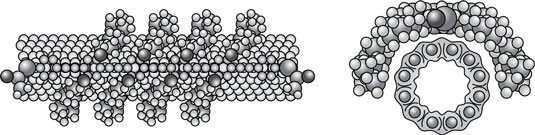
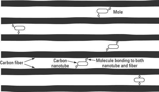
When you include functionalized nanoparticles in a composite material, those nanoparticles can form covalent bonds with the primary material used in the composite. For example, functionalized nanotubes can bond with polymers to produce a stronger plastic. In a carbon fiber composite, functionalized nanotubes bond with the carbon fibers to create a stronger structure.
Nanocomposites are being used in several applications:
-
A variety of nanoparticles such as buckyballs, nanotubes, and silica nanoparticles are being used with various fibers to form nanocomposites used in sports equipment such as tennis racquets to improve their strength or stiffness while keeping them lightweight.
-
Nanocomposites using carbon nanotubes and polymers are being developed to make lighter-weight spacecraft.
-
Nanocomposites using carbon nanotubes in an epoxy are being used to make windmill blades longer, enabling the windmill to generate more electricity.
-
Nanoparticles of clay are used in plastic composites to reduce the leakage of carbon dioxide from plastic bottles, improving the shelf life of carbonated beverages.
-
Composites of nanoparticles and polymers are being developed to produce lightweight, strong plastics to replace metals in cars.
VSEPR MODEL
-
Predicting the Shapes of Molecules
There is no direct relationship between the formula of a compound and the shape of its molecules. The shapes of these molecules can be predicted from their Lewis structures, however, with a model developed about 30 years ago, known as the valence-shell electron-pair repulsion (VSEPR) theory.
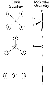
The VSEPR theory assumes that each atom in a molecule will achieve a geometry that minimizes the repulsion between electrons in the valence shell of that atom. The five compounds shown in the figure below can be used to demonstrate how the VSEPR theory can be applied to simple molecules.
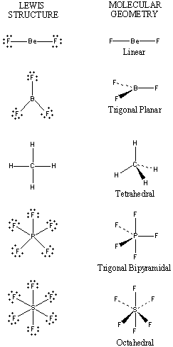
There are only two places in the valence shell of the central atom in BeF2 where electrons can be found. Repulsion between these pairs of electrons can be minimized by arranging them so that they point in opposite directions. Thus, the VSEPR theory predicts that BeF2 should be a linear molecule, with a 180o angle between the two Be-F bonds.

There are three places on the central atom in boron trifluoride (BF3) where valence electrons can be found. Repulsion between these electrons can be minimized by arranging them toward the corners of an equilateral triangle. The VSEPR theory therefore predicts a trigonal planar geometry for the BF3 molecule, with a F-B-F bond angle of 120o.

BeF2 and BF3 are both two-dimensional molecules, in which the atoms lie in the same plane. If we place the same restriction on methane (CH4), we would get a square-planar geometry in which the H-C-H bond angle is 90o. If we let this system expand into three dimensions, however, we end up with a tetrahedral molecule in which the H-C-H bond angle is 109o28′.

Repulsion between the five pairs of valence electrons on the phosphorus atom in PF5 can be minimized by distributing these electrons toward the corners of a trigonal bipyramid. Three of the positions in a trigonal bipyramid are labeled equatorial because they lie along the equator of the molecule. The other two are axial because they lie along an axis perpendicular to the equatorial plane. The angle between the three equatorial positions is 120o, while the angle between an axial and an equatorial position is 90o.

There are six places on the central atom in SF6 where valence electrons can be found. The repulsion between these electrons can be minimized by distributing them toward the corners of an octahedron. The term octahedron literally means “eight sides,” but it is the six corners, or vertices, that interest us. To imagine the geometry of an SF6 molecule, locate fluorine atoms on opposite sides of the sulfur atom along the X, Y, and Z axes of an XYZ coordinate system.

Incorporating Double and Triple Bonds Into the VSEPR Theory
Compounds that contain double and triple bonds raise an important point: The geometry around an atom is determined by the number of places in the valence shell of an atom where electrons can be found, not the number of pairs of valence electrons. Consider the Lewis structures of carbon dioxide (CO2) and the carbonate (CO32-) ion, for example.
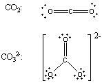
There are four pairs of bonding electrons on the carbon atom in CO2, but only two places where these electrons can be found. (There are electrons in the C=O double bond on the left and electrons in the double bond on the right.) The force of repulsion between these electrons is minimized when the two C=O double bonds are placed on opposite sides of the carbon atom. The VSEPR theory therefore predicts that CO2 will be a linear molecule, just like BeF2, with a bond angle of 180o.
The Lewis structure of the carbonate ion also suggests a total of four pairs of valence electrons on the central atom. But these electrons are concentrated in three places: The two C-O single bonds and the C=O double bond. Repulsions between these electrons are minimized when the three oxygen atoms are arranged toward the corners of an equilateral triangle. The CO32- ion should therefore have a trigonal-planar geometry, just like BF3, with a 120o bond angle.
The Role of Nonbonding Electrons in the VSEPR Theory
The valence electrons on the central atom in both NH3 and H2O should be distributed toward the corners of a tetrahedron, as shown in the figure below. Our goal, however, isn’t predicting the distribution of valence electrons. It is to use this distribution of electrons to predict the shape of the molecule. Until now, the two have been the same. Once we include nonbonding electrons, that is no longer true.
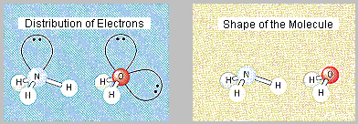
The VSEPR theory predicts that the valence electrons on the central atoms in ammonia and water will point toward the corners of a tetrahedron. Because we can’t locate the nonbonding electrons with any precision, this prediction can’t be tested directly. But the results of the VSEPR theory can be used to predict the positions of the nuclei in these molecules, which can be tested experimentally. If we focus on the positions of the nuclei in ammonia, we predict that the NH3 molecule should have a shape best described as trigonal pyramidal, with the nitrogen at the top of the pyramid. Water, on the other hand, should have a shape that can be described as bent, or angular. Both of these predictions have been shown to be correct, which reinforces our faith in the VSEPR theory.
When we extend the VSEPR theory to molecules in which the electrons are distributed toward the corners of a trigonal bipyramid, we run into the question of whether nonbonding electrons should be placed in equatorial or axial positions. Experimentally we find that nonbonding electrons usually occupy equatorial positions in a trigonal bipyramid. To understand why, we have to recognize that nonbonding electrons take up more space than bonding electrons. Nonbonding electrons need to be close to only one nucleus, and there is a considerable amount of space in which nonbonding electrons can reside and still be near the nucleus of the atom. Bonding electrons, however, must be simultaneously close to two nuclei, and only a small region of space between the nuclei satisfies this restriction.
Because they occupy more space, the force of repulsion between pairs of nonbonding electrons is relatively large. The force of repulsion between a pair of nonbonding electrons and a pair of bonding electrons is somewhat smaller, and the repulsion between pairs of bonding electrons is even smaller.
The figure below can help us understand why nonbonding electrons are placed in equatorial positions in a trigonal bipyramid.
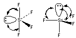
If the nonbonding electrons in SF4 are placed in an axial position, they will be relatively close (90o) to three pairs of bonding electrons. But if the nonbonding electrons are placed in an equatorial position, they will be 90o away from only two pairs of bonding electrons. As a result, the repulsion between nonbonding and bonding electrons is minimized if the nonbonding electrons are placed in an equatorial position in SF4.
The results of applying the VSEPR theory to SF4, ClF3, and the I3– ion are shown in the figure below.
When the nonbonding pair of electrons on the sulfur atom in SF4 is placed in an equatorial position, the molecule can be best described as having a see-saw or teeter-totter shape. Repulsion between valence electrons on the chlorine atom in ClF3 can be minimized by placing both pairs of nonbonding electrons in equatorial positions in a trigonal bipyramid. When this is done, we get a geometry that can be described as T-shaped. The Lewis structure of the triiodide (I3–) ion suggests a trigonal bipyramidal distribution of valence electrons on the central atom. When the three pairs of nonbonding electrons on this atom are placed in equatorial positions, we get a linear molecule.
Molecular geometries based on an octahedral distribution of valence electrons are easier to predict because the corners of an octahedron are all identical.
Intermolecular Interactions in the Gas Phase
Interactions between two or more molecules are called intermolecular interactions, while the interactions between the atoms within a molecule are called intramolecular interactions. Intermolecular interactions occur between all types of molecules or ions in all states of matter. They range from the strong, long-distance electrical attractions and repulsions between ions to the relatively weak dispersion forces which have not yet been completely explained. The various types of interactions are classified as (in order of decreasing strength of the interactions):
ion – ion
ion – dipole
dipole – dipole
ion – induced dipole
dipole – induced dipole
dispersion forces
Without these interactions, the condensed forms of matter (liquids and solids) would not exist except at extremely low temperatures. We will explore these various forces and interactions in the gas phase to understand why some materials vaporize at very low temperatures, and others persist as solids or liquids to extremely high temperatures.
The interactions between ions (ion – ion interactions) are the easiest to understand: like charges repel each other and opposite charges attract. These Coulombic forces operate over relatively long distances in the gas phase. The force depends on the product of the charges (Z1, Z2) divided by the square of the distance of separation (d2):
F = – Z1Z2/d2
Two oppositely-charged particles flying about in a vacuum will be attracted toward each other, and the force becomes stronger and stronger as they approach until eventually they will stick together and a considerable amount of energy will be required to separate them. They form an ion-pair, a new particle which has a positively-charged area and a negatively-charged area. There are fairly strong interactions between these ion pairs and free ions, so that these the clusters tend to grow, and they will eventually fall out of the gas phase as a liquid or solid (depending on the temperature).
Ion – Ion Interactions in the Gas Phase

Let’s go back to that first ion pair which was formed when the positive ion and the negative ion came together. If the electronegativities of the elements are sufficiently different (like an alkali metal and a halide), the charges on the paired ions will not change appreciably – there will be a full electron charge on the blue ion and a full positive charge on the red ion. The bond formed by the attraction of these opposite charges is called an ionic bond. If the difference in electronegativity is not so great, however, there will be some degree of sharing of the electrons between the two atoms. The result is the same whether two ions come together or two atoms come together:
Polar Molecule


The combination of atoms or ions is no longer a pair of ions, but rather a polar molecule which has a measureable dipole moment. The dipole moment (D) is defined as if there were a positive (+q) and a negative (-q) charge separated by a distance (r):
D = qr
If there is no difference in electronegativity between the atoms (as in a diatomic molecule such as O2 or F2) there is no difference in charge and no dipole moment. The bond is called acovalent bond, the molecule has no dipole moment, and the molecule is said to be non-polar. Bonds between different atoms have different degrees of ionicity depending on the difference in the electronegativities of the atoms. The degree of ionicity may range from zero (for a covalent bond between two atoms with the same electronegativity) to one (for an ionic bond in which one atom has the full charge of an electron and the other atom has the opposite charge). In some cases, two or more partially ionic bonds arranged symmetrically around a central atom may mutually cancel each other’s polarity, resulting in a non-polar molecule. An example of this is seen in the carbon tetrachloride (CCl4) molecule. There is a substantial difference between the electronegativities of carbon (2.55) and chlorine (3.16), but the four chlorine atoms are arranged symmetrically about the carbon atom in atetrahedral configuration, and the molecule has zero dipole moment. Saturated hydrocarbons (CnHn+2) are non-polar molecules because of the small difference in the electronegativities of carbon and hydrogen plus the near symmetry about each carbon atom.
Non-polar Molecule

Polar molecules can interact with ions:

or with other polar molecules:

The charges on ions and the charge separation in polar molecules explain the fairly strong interactions between them, with very strong ion – ion interactions, weaker ion – dipole interactions, and considerably weaker dipole – dipole interactions. Even in a non-polar molecule, however, the valence electrons are moving around and there will occasionally be instances when more are on one side of the molecule than on the other. This gives rise to fluctuating or instantaneous dipoles:
Fluctuating Dipole in a Non-polar Molecule

These instantaneous dipoles may be induced and stabilized as an ion or a polar molecule approaches the non-polar molecule.
Ion – Induced Dipole Interaction

Dipole – Induced Dipole Interaction

top
Interactions between ions, dipoles, and induced dipoles account for many properties of molecules – deviations from ideal gas behavior in the vapor state, and the condensation of gases to the liquid or solid states. In general, stronger interactions allow the solid and liquid states to persist to higher temperatures. However, non-polar molecules show similar behavior, indicating that there are some types of intermolecular interactions that cannot be attributed to simple electrical attractions. These interactions are generally called dispersion forces. Electrical forces operate when the molecules are several molecular diameters apart, and become stronger as the molecules or ions approach each other. Dispersion forces are very weak until the molecules or ions are almost touching each other, as in the liquid state. These forces appear to increase with the number of “contact points” with other molecules, so that long non-polar molecules such as n-octane (C8H18) may have stronger intermolecular interactions than very polar molecules such as water (H2O), and the boiling point of n-octane is actually higher than that of water.
Dispersion Forces

It is possible that these forces arise from the fluctuating dipole of one molecule inducing an opposing dipole in the other molecule, giving an electrical attraction. It is also possible that these interactions are due to some sharing of electrons between the molecules in “intermolecular orbitals“, similar to the “molecular orbitals” in which electrons from two atoms are shared to form a chemical bond. These dispersion forces are assumed to exist between all molecules and/or ions when they are sufficiently close to each other. The stronger farther-reaching electrical forces from ions and dipoles are considered to operate in addition to these forces.
Chemical Bond Types

An ionic bond is formed by the attraction of oppositely charged atoms or groups of atoms. When an atom (or group of atoms) gains or loses one or more electrons, it forms an ion. Ions have either a net positive or net negative charge. Positively charged ions are attracted to the negatively charged ‘cathode’ in an electric field and are called cations. Anions are negatively charged ions named as a result of their attraction to the positive ‘anode’ in an electric field.
Every ionic chemical bond is made up of at least one cation and one anion.
Ionic bonding is typically described to students as being the outcome of the transfer of electron(s) between two dissimilar atoms. The Lewis structure below illustrates this concept.

For binary atomic systems, ionic bonding typically occurs between one metallic atom and one nonmetallic atom. The electronegativity difference between the highly electronegative nonmetal atom and the metal atom indicates the potential for electron transfer.
Sodium chloride (NaCl) is the classic example of ionic bonding. Ionic bonding is not isolated to simple binary systems, however. An ionic bond can occur at the center of a large covalently bonded organic molecule such as an enzyme. In this case, a metal atom, like iron, is both covalently bonded to large carbon groups and ionically bonded to other simpler inorganic compounds (like oxygen). Organic functional groups, like the carboxylic acid group depicted below, contain covalent bonding in the carboxyl portion of the group (HCOO) which itself serves as the anion to the acidic hydrogen ion (cation).

A covalent chemical bond results from the sharing of electrons between two atoms with similar electronegativities A single covalent bond represent the sharing of two valence electrons (usually from two different atoms). The Lewis structure below represents the covalent bond between two hydrogen atoms in a H2 molecule.
|
|
|
|
Dot Structure
|
Line Structure
|
Multiple covalent bonds are common for certain atoms depending upon their valence configuration. For example, a double covalent bond, which occurs in ethylene (C2H4), results from the sharing of two sets of valence electrons. Atomic nitrogen (N2) is an example of a triple covalent bond.
Double Covalent Bond

Triple Covalent Bond
|
|
|
The polarity of a covalent bond is defined by any difference in electronegativity the two atoms participating. Bond polarity describes the distribution of electron density around two bonded atoms. For two bonded atoms with similar electronegativities, the electron density of the bond is equally distributed between the two atom is This is anonpolar covalent bond. The electron density of a covalent bond is shifted towards the atom with the largest electronegativity. This results in a net negative charge within the bond favoring the more electronegative atom and a net positive charge for the least electronegative atom. This is a polar covalent bond.

A coordinate covalent bond (also called a dative bond) is formed when one atom donates both of the electrons to form a single covalent bond. These electrons originate from the donor atom as an unshared pair.

Both the ammonium ion and hydronium ion contain one coordinate covalent bond each. A lone pair on the oxygen atom in water contributes two electrons to form a coordinate covalent bond with a hydrogen ion to form the hydronium ion. Similarly, a lone pair on nitrogen contributes 2 electrons to form the ammonium ion. All of the bonds in these ions are indistinguishable once formed, however.
 |
 |
|
Ammonium (NH4+)
|
Hydronium (H3O+)
|
Some elements form very large molecules by forming covalent bonds. When these molecules repeat the same structure over and over in the entire piece of material, the bonding of the substance is called network covalent. Diamond is an example of carbon bonded to itself. Each carbon forms 4 covalent bonds to 4 other carbon atoms forming one large molecule the size of each crystal of diamond.

Silicates, [SiO2]x also form these network covalent bonds. Silicates are found in sand, quartz, and many minerals.

The valence electrons of pure metals are not strongly associated with particular atoms. This is a function of their low ionization energy. Electrons in metals are said to be delocalized (not found in one specific region, such as between two particular atoms).
Since they are not confined to a specific area, electrons act like a flowing “sea”, moving about the positively charged cores of the metal atoms.
- Delocalization can be used to explain conductivity, malleability, and ductility.
- Because no one atom in a metal sample has a strong hold on its electrons and shares them with its neighbors, we say that they are bonded.
- In general, the greater the number of electrons per atom that participate in metallic bonding, the stronger the metallic bond.
Bonds
So far, we’ve studied atoms and compounds and how they react with each other. Now let’s take a look at how these atoms and molecules hold together. Bonds hold atoms and molecules of substances together. There are several different kinds of bonds; the type of bond seen in elements and compounds depends on the chemical properties as well as the attractive forces governing the atoms and molecules. The three types of chemical bonds are Ionic bonds, Covalent bonds, and Polar covalent bonds. Chemists also recognize hydrogen bonds as a fourth form of chemical bond, though their properties align closely with the other types of bonds.
In order to understand bonds, you must first be familiar with electron properties, including valence shell electrons. The valence shell of an atom is the outermost layer (shell) of an electron. Though today scientists generally agree that electrons do not rotate around the nucleus, it was thought throughout history that each electron orbited the nucleus of an atom in a separate layer (shell). Today, scientists have concluded that electrons hover in specific areas of the atom and do not form orbits; however, the valence shell is still used to describe electron availability.
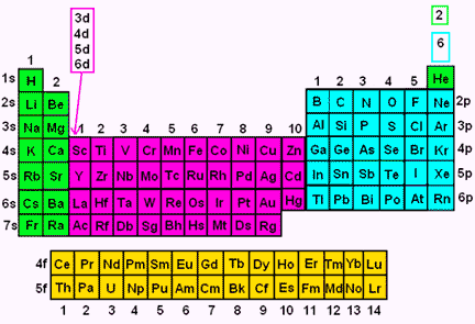
One can determine how many electrons an atom will have by looking at its periodic properties. In order to determine an element’s periodic properties, you will need to locate a periodic table. After you’ve found your periodic table, look at the roman numerals above each column of the table. You should see that above Hydrogen, there’s a IA, above Beryllium there’s a IIA, above Boron there’s a IIIA, and so on all the way to Fluorine, which is VIIA. Also, note that the metals are all in group B—their roman numerals have the letter B afterwards instead of the letter A. For now, we are going to ignore the columns with a B, and focus on the columns with an A (the non-metals, generally speaking). Once you have located the group-A elements, we are going to count across, giving each column a number, like this:
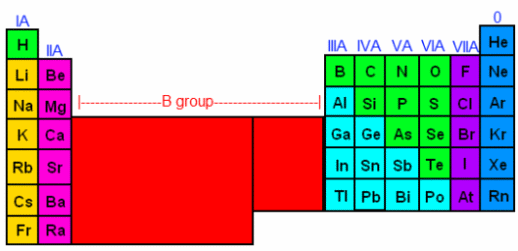
The first A-column is I (1), then counting across, 2-8 (skipping the B group, which consists of metals). In the periodic table we labeled the 8th column as 0, however when counting electrons, we’ll count it as 8. Now, we can determine how many valence electrons each element has in its outermost shell. The elements in the IA column have 1 valence electron. The elements in the IIA column have 2 bonding electrons, and so on. By the time we get to the noble gases (the column labeled 0), we are up to 8 bonding electrons. This means that these gases can stand on their own, or donate electrons to another element, but they cannot accept any more electrons. This is because the electrons they have satisfy the octet rule.
The Octet and Duet Rules
When it comes to bonding, everything is based on how many electrons an element has or shares with its compound partner or partners. The octet rule is followed by most elements, and it says that to be stable, an atom needs to have eight electrons in its outermost shell. Elements that do not follow the octet rule are H, He, B, Li and Be (sometimes). Lithium gives up an electron whereas the other elements listed here gain one. These elements instead follow the duet rule which says that the atoms only need two valence electrons to be stable. When bonding, stability is always considered and preferred. Therefore, atoms bond in order to become more stable than they already are.
Not all atoms bond the same way, so we need to learn the different types of bonds that atoms can form. There are three (sometimes four) recognized chemical bonds; they are ionic, covalent, polar covalent, and (sometimes) hydrogen bonds.
Ionic Bonds
Ionic bonds form when two atoms have a large difference in electronegativity. (Electronegativity is the quantitative representation of an atom’s ability to attract an electron to itself). Although scientists do not have an exact value to signal an ionic bond, the amount is generally accepted as 1.7 and over to qualify a bond as ionic. Ionic bonds often occur between metals and salts; chloride is often the bonding salt. Compounds displaying ionic bonds form ionic crystals in which ions of positive and negative charges hover near each other, but there is not always a direct 1-1 correlation between positive and negative ions. Ionic bonds can typically be broken through hydrogenation, or the addition of water to a compound.
Covalent Bonds
Covalent bonds form when two atoms have a very small (nearly insignificant) difference in electronegativity. The value of difference in electronegativity between two atoms in a covalent bond is less than 1.7. Covalent bonds often form between similar atoms, nonmetal to nonmetal or metal to metal. Covalent bonding signals a complete sharing of electrons. There is usually a direct correlation between positive and negative ions, meaning that because they share electrons, the atoms balance. Covalent bonds are usually strong because of this direct bonding.
Polar Covalent Bonds
Polar covalent bonds fall between ionic and covalent bonds. They result when two elements bond with a moderate difference in electronegativity moderately to greatly, but they do not surpass 1.7 in electronegativity difference. Although polar covalent bonds are classified as covalent, they do have significant ionic properties. They also induce dipole-dipole interactions, where one atom becomes slightly negative and the other atom becomes slightly positive. However, the slight change in charge is not large enough to classify it entirely as an ion; they are simply considered slightly positive or slightly negative. Polar covalent bonds often indicate polar molecules, which are likely to bond with other polar molecules but are unlikely to bond with non-polar molecules.
Hydrogen Bonds
Hydrogen bonds only form between hydrogen and oxygen (O), nitrogen (N) or fluorine (F). Hydrogen bonds are very specific and lead to certain molecules having special properties due to these types of bonds. Hydrogen bonding sometimes results in the element that is not hydrogen (oxygen, for example) having a lone pair of electrons on the atom, making it polar. Lone pairs of electrons are non-bonding electrons that sit in twos (pairs) on the central atom of the compound. Water, for example, exhibits hydrogen bonding and polarity as a result of the bonding. This is shown in the diagram below.
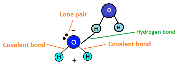
Because of this polarity, the oxygen end of the molecule would repel negative atoms like itself, while attracting positive atoms, like hydrogen. Hydrogen, which becomes slightly positive, would repel positive atoms (like other hydrogen atoms) and attract negative atoms (such as oxygen atoms). This positive and negative attraction system helps water molecules stick together, which is what makes the boiling point of water high (as it takes more energy to break these bonds between water molecules).
In addition to the four types of chemical bonds, there are also three categories bonds fit into: single, double, and triple. Single bonds involve one pair of shared electrons between two atoms. Double bonds involve two pairs of shared electrons between two atoms, and triple bonds involve three pairs of shared electrons between two atoms. These bonds take on different natures due to the differing amounts of electrons needed and able to be given up.
Now, let’s look at determining what types of bonds we see in different compounds. We’ve already looked at the bonds in H2O, which we determined to be hydrogen bonds. However, now let’s look at a few other types of bonds as examples.
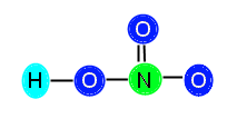
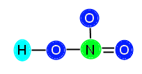
Compound: HNO3 (also known as Nitric acid)
There are two different determinations we can make as to what these bonds look like; first we can decide whether the bonds are covalent, polar covalent, ionic, or hydrogen. Then, we can determine if the bonds are single, double, or triple.
In order to decide whether the bonds are covalent, polar covalent, ionic or hydrogen, we need to look at the types of elements seen and the electronegativity values. We look at the elements and see hydrogen, nitrogen, and oxygen—no metals. This rules out ionic bonding as a type of bond seen in the compound. Then, we would look at electronegativity values for nitrogen and oxygen. Oftentimes, this information can be found on a periodic table, in a book index, or an educational online resource. The electronegativity value for oxygen is 3.5 and the electronegativity value for nitrogen is 3.0. The way to determine the bond type is by taking the difference between the two numbers (subtraction). 3.5 – 3.0 = 0.5, so we can determine that the bond between nitrogen and oxygen is a covalent bond. We can also determine, from past knowledge, that the bond between oxygen and hydrogen is a hydrogen bond as it was in water.
Now, we need to count the electrons and draw the diagram for HNO3. For more help counting electrons, please see the page onElectron Configuration. For more help drawing the Lewis structures, please see the page on Lewis Structures. This process combines both of these in order to determine the structure and shape of a molecule of the compound.
First, we determine that N follows the octet rule, so it needs eight surrounding electrons. This is important to keep in mind as we move forward. Next we count up how many valence electrons the compound has as a whole. H gives us 1, N gives us 5, and each O gives us 6. We can discern this from looking at the tops of the columns in the periodic table (see above). We then add these numbers together (3 x 6 = 18, + 1 = 19, + 5 = 24), and we get 24 electrons that we need to distribute throughout the molecule. First, we need to draw the molecule to see how many initial bonds we’ll be putting in. Our preliminary structure looks like this:

Now, we can count how many electrons we have used by counting 2 electrons for each bond placed. We see that we have placed 4 bonds, so we have used 8 electrons. 24 – 8 = 16 electrons that we need to distribute. In order to correctly place the rest of the electrons, we need to determine how many electrons each atom needs to be stable.
The central atom, N, has three bonds attached (equivalent of 6 electrons) so it needs 2 more electrons to be stable. The O to the right has one bond (two electrons) so it needs 6 more to be stable. The O above the N has one bond (two electrons) so it also needs 6 electrons to be stable. The O to the left of the N is bonded both to N and to H, so it has two bonds (4 electrons); therefore, it needs 4 more electrons to be stable. We add up the total amount of electrons needed, 2 + 6 + 6 + 4 = 18, and see that we need 18 electrons to stabilize the compound. We know this is not possible, since we only have 16 available electrons. When this happens, we need to insert a double bond in order to resolve the problem of lack of electrons. This is because, although we count each bond as 2 electrons, the elements joined together in the bond are actually sharing the electrons. Therefore, when we count out the bonds, we are counting some electrons twice because they are shared. This is normal and expected, and resolves not having enough valence electrons. Now, we need to decide where to put the double bond in this compound. We know that the double bond cannot go between O and H, because H does not have enough room to accept another electron. Therefore, we know we must place the bond between N and O. You might be thinking, how do I decide where to put the bond? In this particular example, we can place the bond either between the top O and N, or the right O and N. This is because HNO3 displays resonance.
Here are the ways you can place the double bond:
or
We are going to keep the bond between N and the right O in our example. After we add in the bond, we subtract two more electrons from our available electrons (16) and are left with 14 electrons to distribute. Now we need to make sure we have the correct number of electrons. After placing in the double bond, N is now stable because it has 4 bonds (8 electrons) surrounding it. It does not need any additional electrons. The top O (above N) needs 6 electrons, the right O now only needs 4 electrons (because it has a double bond now, which is 4 electrons), and the left O still needs 4 electrons to become stable. We add these numbers together, 6 + 4 + 4 = 14, and we see that 14 is the number of electrons we have, so we can go ahead and distribute them, like this:
Now, our compound is stable with appropriately distributed valence electrons. We can see that there are three single bonds (H—O, N—O, and N—O) and one double bond (N==O).
Electron Configuration
Electrons play a crucial role in chemical reactions and how compounds interact with each other. Remember, electrons are the negative particles in an atom that “orbit” the nucleus. Although we say they orbit the nucleus, we now know that they are actually in a random state of motion surrounding the nucleus rather than making circles around it, which is what an orbit implies. The best analogy to describe electron motion within an atom is how bees buzz around a beehive. They don’t fly in complete circles around it, but they do hover and move around it in a seemingly random motion.
Electrons increase in elements as protons do, which is from left to right and from top to bottom on the periodic table. Therefore, the element with the fewest electrons would be in the top left-hand corner of the table and the element with the most electrons would be in the bottom right hand corner. The elements are arranged so that the increase from element to element is one electron. Therefore, in the first row, we see hydrogen and helium. This is because hydrogen has one electron and helium has two electrons, so we place them in ascending order.
Electron Orbitals
We categorize electrons according to what orbital level in which they reside. The four orbitals are s, p, d, and f. They are classified by divisions on the periodic table, as follows:
The first orbital is the s orbital. It has room to hold two electrons. The electrons have opposite spins, so it makes sense that they are paired together. The s orbital is a sphere, with the x, y, and z axes passing through it, like this:
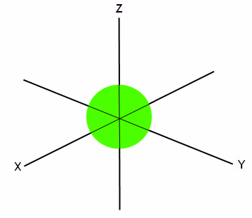
This means that the two electrons can occupy any of the space seen in this sphere, and they sort of “hover” around in the given space.
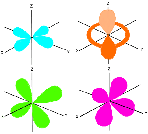
The next orbital is the p orbital. It can hold up to six electrons, therefore it has three sub-orbitals (each can hold two electrons). The spins on electrons are still opposite, this time split into three and three (since the first orbital only held two electrons, we said the spins were opposite. Now that this orbital can hold six electrons, three spin one way and three spin the opposite way). The p orbital is not sphere shaped, however it does have six lobes that are shaped like balloons. Two lobes are on the x axis, two are on the y axis, and two are on the z axis. These three separations are considered sub-orbitals and combine to make up the entire p orbital. The nucleus of the atom is located where these three axes meet. The p orbital looks like this:
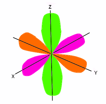
The next orbital is the d orbital. It can hold up to 10 electrons, therefore it has five sub-orbitals (each can hold two electrons). The spins of the electrons are opposite, so five are spinning one way and the other five are spinning the opposite way. The d orbital is not sphere shaped; it looks more like the p orbital, except there are more lobes that cannot be shown all at once. We showed the entire p orbital (all three of the sub-orbitals) in one diagram, because there were two lobes on each axis. However, we need to show the five different sub-orbitals of the d orbital in order to fully explain where the lobes are located, and how they are shaped. We will show you four views, with labels on all of the axes.
The first view is of the lobes that lie on the XY plane, shown in aqua here. The second view is a three dimensional view of lobes on the Z axis that rotate 360 degrees around the axis. There are two lobes, one in the top hemisphere and one in the bottom, and a tube-shaped area that circles the Z axis and intersects the X and Y axes. It’s shown here in orange. The third view is of the lobes on the ZY plane, with the X axis running perpendicular to it. It’s shown here in green. The last view is of the lobes lying on the ZX plane, and is shown here in pink. If all of these layers were put together, we would see a sort of star-burst image, with a tube encircling the middle.
The final orbital is the f orbital, and scientists are not completely sure of the shape of its orbital. However, they do have seemingly accurate predictions of where electrons will fall. We will show you the following probabilities of where electrons lie:
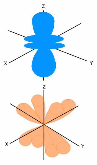
We showed you two probabilities of where the f orbitals lie; however, the first image (in blue) is shown on the Z axis. It is actually repeated on the X axis and again on the Y axis. The second image (in orange) is shown in the XYZ dimensions; however, it is repeated three more times for a total of four positions using this shape and lobe configuration. We say that these are probable locations because scientists cannot actually track and determine the exact location of electrons. However, through research and abilities to track electrons in other orbitals, scientists can say that the likely location of f-level electrons is in one of these locations.
Diagonal Rule, or Madelung’s Rule
In chemistry, the Diagonal Rule (also known as Madelung’s Rule) is a guideline explaining the order in which electrons fill the orbital levels. The 1s2 orbital is always filled first, and it can contain 2 electrons. Then the 2s2 level is filled, which can also hold 2 electrons. After that, electrons begin to fill the 2p6 orbital, and so on. The diagonal rule provides a rule stating the exact order in which these orbitals are filled, and looks like this:
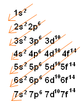
As you can see, the red arrows indicate the filling of orbital levels. Starting at the top, the first red arrow crosses the 1s2 orbital. If you follow these arrows down the list, you can easily determine the order that electrons fill the orbital levels.
There is an exception to this rule when filling the orbitals of heavier electrons. For example, when filling the 5s2 orbitals, the rule says that 5s2 will fill, and then 4d10 will fill. However, when filling these orbitals for certain metals, only one electron will fill the 5s2 orbital, and the next electron will jump into the 4d10 orbital. This can be predicted, but cannot be exactly determined until it is observed. The same is true for the 6s2 orbital-for certain heavy metals, the 6s2 will only contain one electron, and the other electrons will jump to the 5d10 orbital.
Electron Notation
Following the diagonal rule, there is an easy way to write electron configuration. We are simply going to use the orbital names we learned from the diagonal rule (1s2, 2s2 and so on). However, we are only going to write the number of electrons that the atom actually contains. For example, hydrogen has one electron, which would fall in the 1s orbital. Thus, the electron configuration for hydrogen is 1s1. We write the superscript as 1 because there is one electron. Helium, the next element, contains two electrons. They both fill the 1s orbital, so the electron configuration for helium is 1s2. Here again, we write the superscript as 2 because there are two electrons.
Electron configuration moves across and down the periodic table. You might have noticed that we first put one electron in the 1s orbital (with hydrogen), and then we put two electrons in the 1s orbital (with helium). Continuing this trend, we would next have 3 electrons with lithium. We would place two of them in the 1s orbital, and one of them in the 2s orbital, so the electron configuration would be 1s2 2s1. However, we can also write this using the configuration of helium, because it is a noble gas. Noble gases are stable elements, so we can use their configurations in determining other configurations. So, instead of writing 1s2 2s1, we would write [He] 2s1. This means that lithium contains the same configuration as helium, and then has one more electron in the 2s orbital. Notice that we use brackets to encase the previous noble gas, and then we continue writing the configuration as we normally would. This might not seem like a big deal, or a shortcut right now, but once you get pretty far down the periodic table, this will save you a lot of time and energy.
We’ll show you one short example of this. Let’s say we need to determine the electron configuration for Ba, Barium. Counting across the table, we would come up with the following configuration:
1s2 2s2 2p6 3s2 3p6 4s2 3d 10 4p6 5s2 4d10 5p6 6s2
Instead of writing all of this out, we could simply find the previous noble gas, which is Xe. Therefore, we can write [Xe] and then figure out the rest of the configuration. We look and see that Ba is in the 6th row, so we know that we’re going to start with 6s2. We can look and see that Ba is the second element in that row, so it has two electrons to go in the 6s orbital.
Thus, we can conclude that the final electron configuration for Ba is [Xe] 6s2.
Electron Spin
Every electron placed in an orbital has a feature we refer to as “spin.” We’ve already talked about electrons having been thought to have a specific “orbit,” and then later discovered to hover in the places listed above. Well, electrons don’t literally spin, but their movement sort of looks like someone somersaulting, in a very fast, random state. This is called spin. Each electron can either have a +1/2 spin or a -1/2 spin, which indicates its direction of motion. There is never a 0 spin. When filling orbitals, electrons spin in pairs, one + and one -. The electrons with an up (+) spin fill first, and the electrons with a down (-) spin fill second. It would look like this:
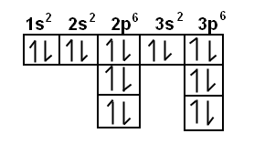
and so on. Because the s orbital can hold two electrons, we draw one box in which two electrons (represented here with arrows) can fit. Since the p orbital can hold 6 electrons, we draw 3 boxes that will each hold 2 electrons. This will continue with the d orbital (10 electrons fit in 5 boxes) and the f orbital (14 electrons fit in 7 boxes).
These boxes fill in a certain order-all of the boxes in one column will fill with up spin electrons first, and then down spin. So, for example, if the element has a configuration of 1s2 2s2 2p3, it would look like this:
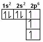
As you can see, we filled the boxes with up arrows (electrons) first. If we had more electrons, we would go back and add them in to the second column, as down spin electrons.
Leave a Reply
Want to join the discussion?Feel free to contribute!